A PCF8574 pin is ready for input only when its output latch contains a 1. The chip has no direction register: writing 1 releases the pin into its quasi-bidirectional high state, while writing 0 actively pulls it low.
Featured image: Adafruit.
This behavior comes directly from Texas Instruments data sheet SCPS068K, revised September 2024. Treating the device like a conventional microcontroller GPIO block can leave a switch apparently stuck low or make an unrelated output update disable an input.
The latch is the direction control
At power-on, all eight I/O latches are high. In that state, each pin has only its quasi-bidirectional current source to VCC, so an external switch or open-drain signal can pull the line low. A port read then reports the physical pin level.
To make P3 an input while keeping P0 and P1 low outputs, for example, the byte written to the device must keep bit 3 at 1. If later code constructs a fresh output byte with bit 3 at 0, it has not merely changed cached data—it has turned P3 into a driven-low output.
The robust pattern is to keep a software shadow byte. Bits assigned to inputs remain 1 in that shadow; only intended output bits are changed. Write the complete shadow byte after an output change, then read the port separately when input state is needed.
Do not use a read-modify-write result blindly
A read returns physical pin levels, not simply the last byte written. Suppose a released input is currently held low by a button. If firmware reads that low bit, modifies an output bit, and writes the whole result back, the button’s zero is written into the latch. After the button opens, the PCF8574 still drives the pin low.
That is why the output shadow must represent intent rather than the latest sampled input. The same rule matters when a library exposes individual pin objects: verify that it preserves released input bits internally instead of rebuilding a byte from the sampled port.
INT reduces polling, but it is not an event queue
The INT pin is open-drain and needs a pull-up. TI states that a rising or falling edge on an input-mode port pin can assert it. Reading or writing the affected port resets and rearms the interrupt circuit; returning the input to its original state also removes the condition.
A safe service sequence is short:
- On INT, perform one port read and save the byte.
- Compare it with the last accepted input state to find changed bits.
- Debounce or validate those changes in software as the application requires.
- Leave every input bit at 1 in the next output-shadow write.
The data sheet also documents a narrow blind spot: an interrupt that occurs during the I2C acknowledge clock can be lost or shortened because reset happens during that pulse. INT therefore tells the host to sample state; it does not preserve a count of every edge. Fast pulse trains and encoders need a counter or hardware designed for edge capture.
Keep voltage and bus speed inside the actual part limits
TI rates the PCF8574 for a 2.5 V to 6 V supply and specifies a maximum I2C clock of 100 kHz. Do not assume that a board sold beside 400 kHz I2C sensors makes the original PCF8574 a Fast-mode device. Configure the bus for the slowest target unless the exact part marking and its data sheet say otherwise.
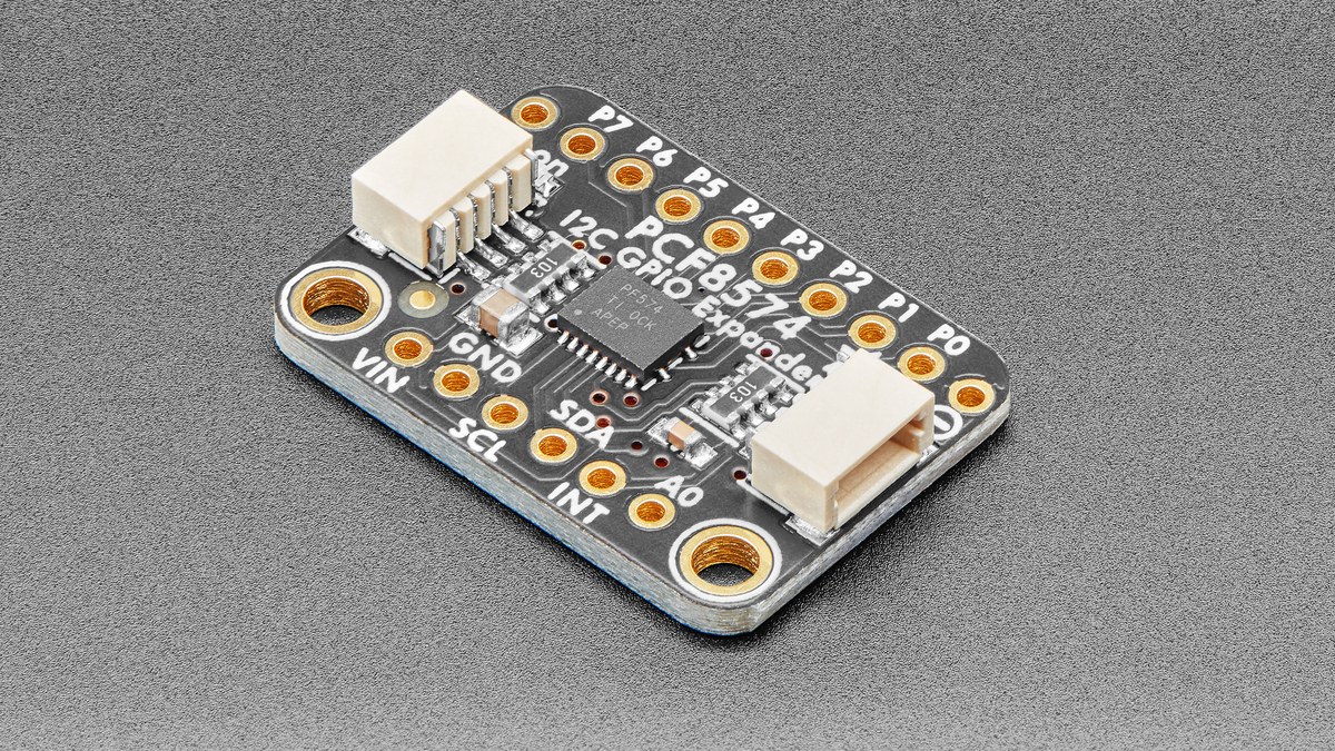
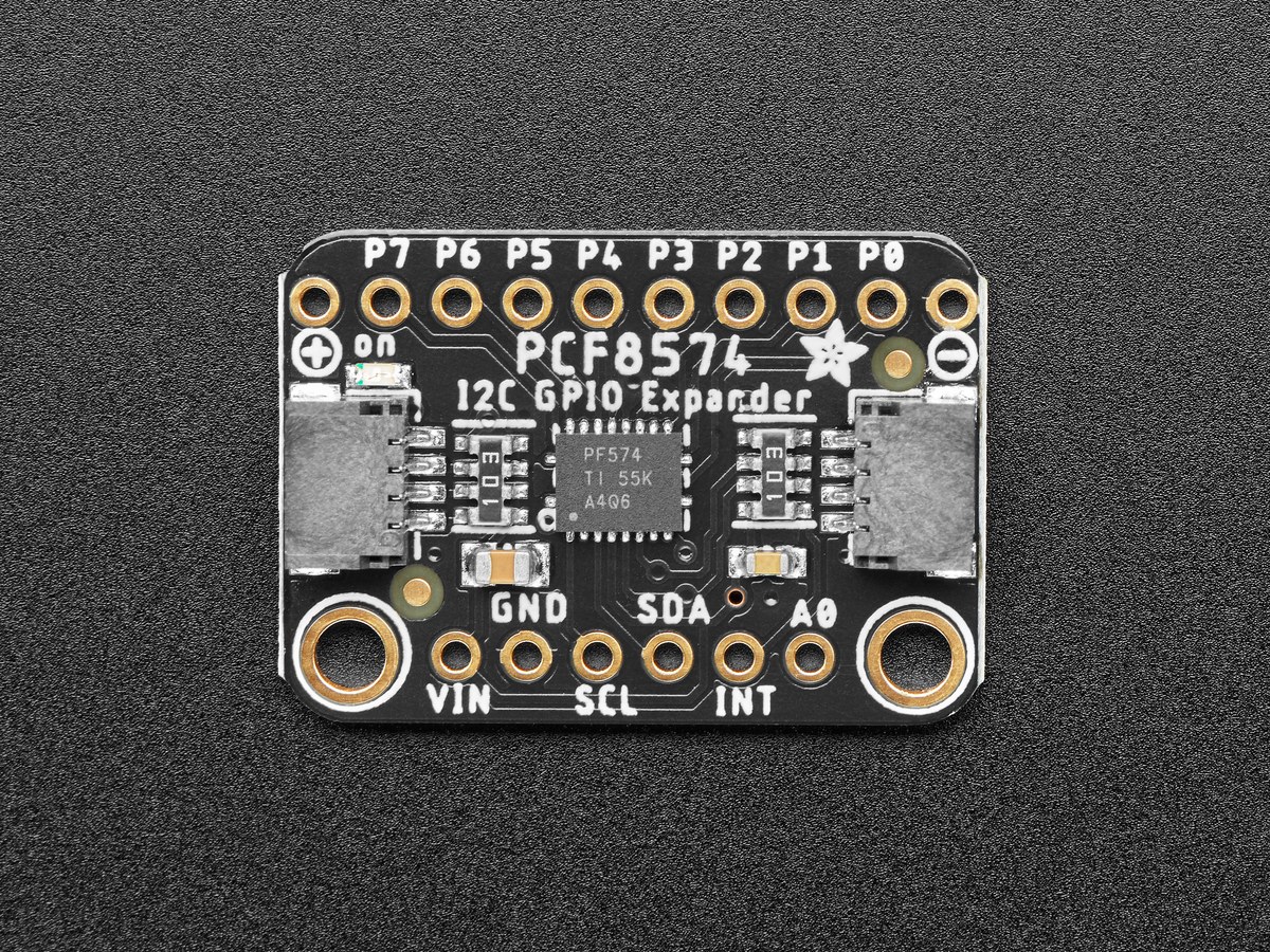
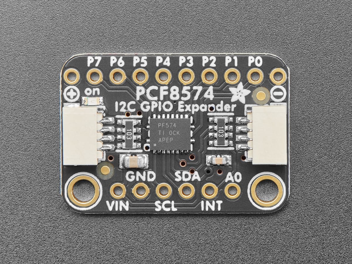
The A0, A1 and A2 inputs select one of eight addresses. The Adafruit breakout adds STEMMA QT connectors, address jumpers and an accessible INT pin, but the underlying latch and interrupt semantics remain those of the PCF8574.
If SDA itself is held low and transactions cannot finish, that is a bus-recovery problem rather than a port-direction problem; use a defined I2C stuck-low recovery sequence before debugging the GPIO byte.