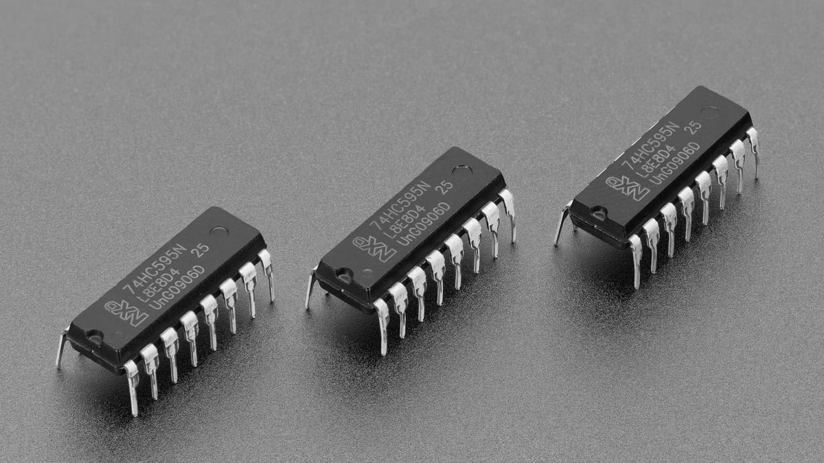
A 74HC595 that flashes random LEDs or energizes outputs while a microcontroller boots usually has an undefined control pin, not a mysterious serial-data problem. Hold OE high so the outputs remain high-impedance, hold SRCLR high so the shift register is not being cleared, and give both clock inputs defined idle levels before firmware configures the GPIO. Then shift a known byte, pulse RCLK, and pull OE low only after the storage register contains the intended startup state.
Featured image: Adafruit.
Why the startup state is exposed
The distinction among those controls matters. The SN74HC595 contains an 8-bit shift register followed by a separate 8-bit storage register. SRCLK advances serial data into the first register; RCLK transfers that pattern to the storage register; OE connects or disconnects the storage register from the output pins. Treating reset, latch and output enable as interchangeable produces exactly the sort of startup glitch that is difficult to reproduce after firmware is running.
Define the four pins that decide startup behavior
Texas Instruments specifies both SRCLK and RCLK as positive-edge triggered. A floating clock can therefore register an unintended edge while the MCU pin is still an input. Add pull-down resistors if the desired idle state is low, or otherwise provide a deterministic level that agrees with the firmware’s initialization sequence.
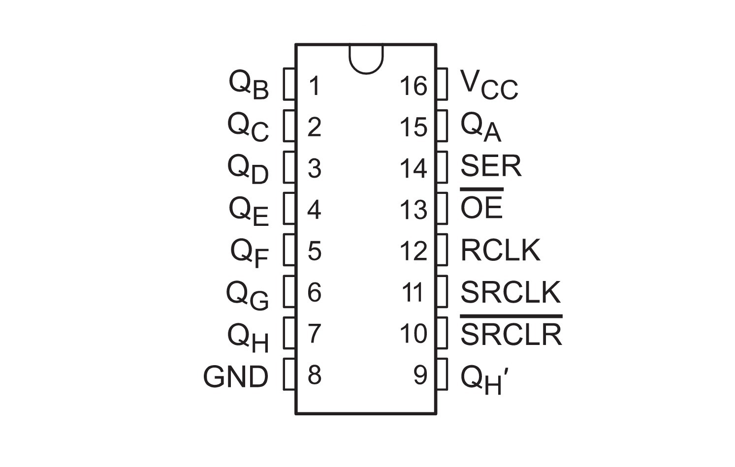
OE is active low. When it is high, QA through QH are high-impedance; the internal storage register is not erased. A pull-up on OE is therefore the cleanest hardware interlock when a brief output pulse could move a motor, switch a relay or expose a power path. Firmware releases the outputs by driving OE low after initialization.
SRCLR is also active low, but it clears the shift register rather than directly blanking the external outputs. To present zeros at QA through QH, the cleared pattern must still be transferred into the storage register with a rising edge on RCLK. Keep SRCLR high during normal shifting; a pull-up prevents an undefined MCU pin from repeatedly clearing incoming data.
SER, the serial input, should also have a known level if the controller can be unpowered or disconnected while clock activity is possible. A pull-down is a common default for an all-zero startup word. The exact resistor value is less important than ensuring it is strong enough to defeat leakage and noise without burdening the GPIO; values around 10 kΩ are a conventional starting point for short, local logic wiring.
Use a release sequence that cannot expose stale bits
A deterministic sequence is short:
- Hardware keeps
OEhigh andSRCLRhigh through reset. - Firmware drives
SRCLKandRCLKlow before changing them to outputs. - Shift eight known bits through
SER, clocking each on the rising edge ofSRCLK. - Pulse
RCLKhigh once to copy the completed byte into the output register. - Drive
OElow to make the known state visible.
Arduino’s shiftOut() reference illustrates the software side: it writes one byte, one bit at a time, using a data pin and clock pin. The latch pulse remains a separate operation. Keeping the latch low during shifting prevents the output register from following intermediate bit patterns.
digitalWrite(oePin, HIGH);      // outputs disabled
digitalWrite(latchPin, LOW);
shiftOut(dataPin, clockPin, MSBFIRST, 0x00);
digitalWrite(latchPin, HIGH);   // known byte reaches storage register
digitalWrite(oePin, LOW);       // outputs enabled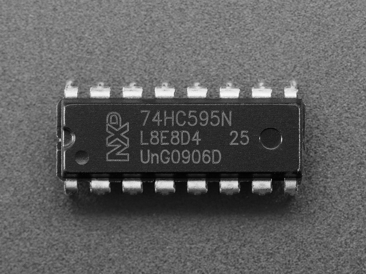
Separate logic glitches from overloaded outputs
If the startup sequence is correct but LEDs still flicker when several outputs turn on, check electrical loading. TI lists the SN74HC595 for a 2 V to 6 V supply and gives 24 MHz as the product-page clock-frequency figure. The page also lists maximum characterized output currents of 7.8 mA sink and −7.8 mA source; those are not permission to drive relays or motors directly. Use current-limiting resistors for LEDs and external transistors or drivers for larger loads.
Also place a local 0.1 µF ceramic bypass capacitor between VCC and GND, close to the package. Simultaneous output switching creates short current transients; a long breadboard power path can turn those into supply dips that resemble a bad clock. Probe VCC at the IC while changing the output pattern if the fault correlates with the number of active channels.
For cascaded 74HC595s, connect QH′ to the next chip’s SER, share the clock and latch lines, and shift the complete chain before the single latch pulse. Keep OE high for the entire transaction when intermediate outputs would be unsafe. The same startup rule scales: first establish a known storage-register pattern, then expose it.
The fastest diagnostic
If a pull-up on OE eliminates the boot glitch, the problem was output exposure during an undefined interval. If unwanted bits still appear after a known byte is shifted and latched, inspect SRCLK and RCLK for extra rising edges and verify that SRCLR remains high. If the logic trace is clean but the supply dips as outputs switch, move to load drive and decoupling. Those three branches—enable timing, clock integrity and electrical load—cover most “random” 74HC595 startup failures without swapping parts blindly.