The DS3502 replaces a 10 kΩ mechanical potentiometer with a 128-position resistor ladder controlled over I²C. That does not make its RW pin a small power supply or a conventional DAC output. It remains the wiper of an analog network, so load current, terminal voltage and startup state still determine whether the circuit behaves as intended.
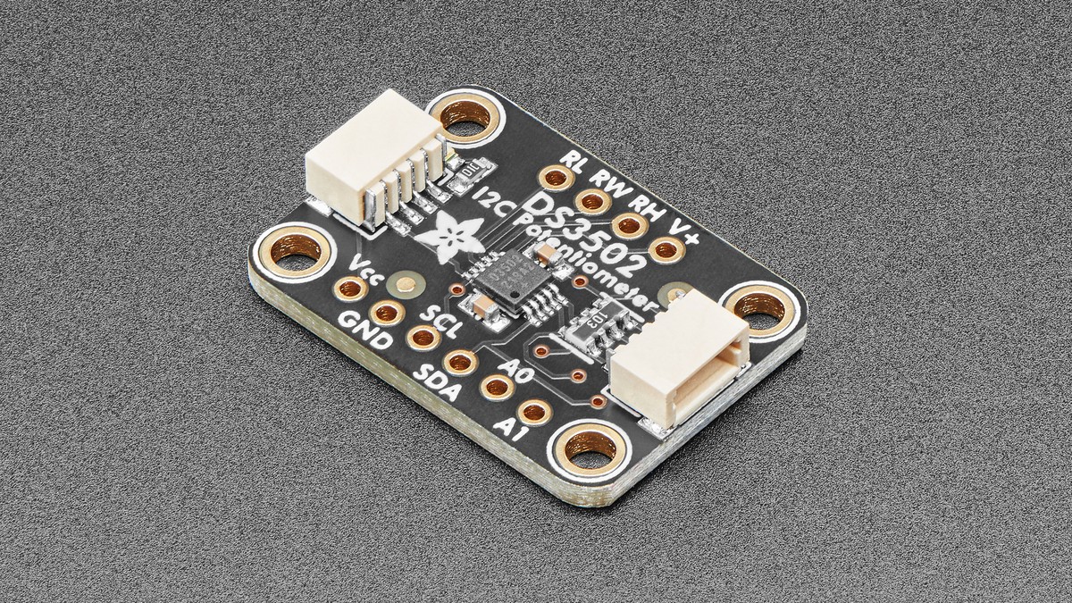
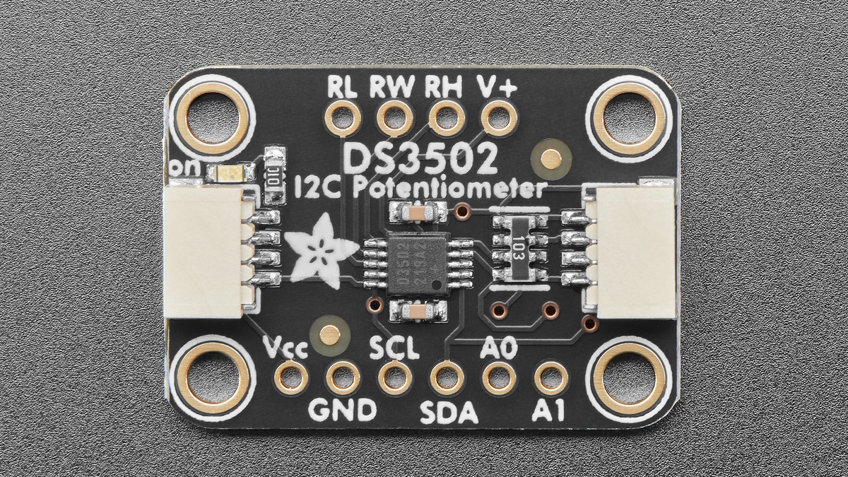
Adafruit’s DS3502 guide exposes the part on a STEMMA QT breakout, but the design decision starts with the three analog terminals: RH, RL and RW. Firmware chooses where RW connects along the ladder; the external circuit decides what voltage or resistance that position produces.
Translate the 7-bit code into a ratio
The wiper register is seven bits, giving positions 0 through 127. For a divider with RH at VH and RL at VL, the unloaded output is approximately VRW = VL + (code/127)(VH − VL). With 5 V across the ladder, one ideal step is about 39 mV. Actual output also includes end resistance, wiper resistance, resistor tolerance and whatever the next stage draws.
That loading term is the common surprise. A meter or op-amp input with very high impedance barely disturbs the divider. A low-resistance load from RW to ground sits in parallel with part of the ladder, bends the code-to-voltage relationship and increases wiper current. The DS3502 belongs in a setpoint, trim or signal path; it should not directly drive a motor, lamp, speaker or other power load.
Logic power and analog terminal voltage are separate constraints
On Adafruit’s breakout, VCC powers the I²C logic and sets its logic level. The analog terminals can handle a higher controlled range: the guide lists 4.5 V to 15.5 V for the analog voltage. When RH is above VCC, the board’s V+ wiper-bias connection must be at the same or a higher voltage than RH. The default solder jumper ties V+ to RH; changing that routing without understanding its purpose can violate the analog switch bias.
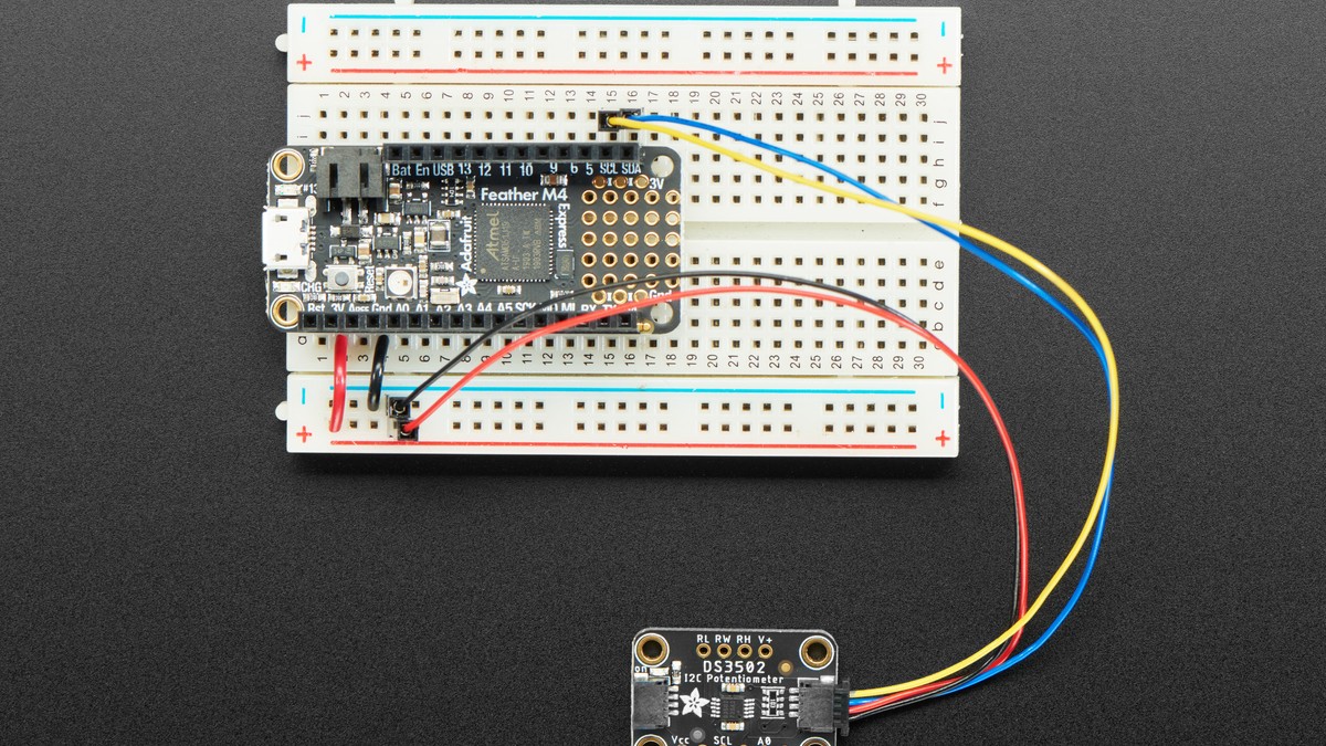
The I²C side is simpler. The breakout includes 10 kΩ pull-ups on SDA and SCL. A0 and A1 select four addresses from 0x28 through 0x2B, and the address pins are sampled at power-up. If firmware changes jumpers while the board is energized, the address does not follow until the part is power-cycled.
Use the nonvolatile default deliberately
The DS3502 can store a default wiper position that is restored on power-up. That is useful when a bias or contrast setting must be valid before the microcontroller finishes booting. It is also a system-state decision: a safe startup value should be written intentionally rather than relying on whichever setting happened to be saved during development.
A digital potentiometer is most predictable when the surrounding circuit would already work with a mechanical 10 kΩ pot and only needs repeatable electronic adjustment. If the requirement is an accurate buffered voltage, bipolar output, high current or monotonic calibration across a heavily loaded node, a DAC plus an amplifier is usually the clearer architecture.